1. Optoelectronic Synaptic Devices
- Materials and Devices:
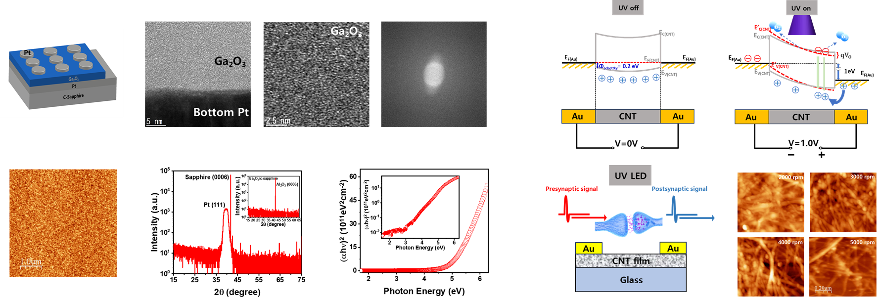
- Focused on developing Pt/Ga₂O₃/Pt memristors and memcapacitors capable of functioning as dual-functional optoelectronic synaptic devices.
- Investigating the role of single-walled carbon nanotube (SWCNT) films for precise optoelectronic response due to their high conductivity and light-sensitive properties.
- Key Findings:
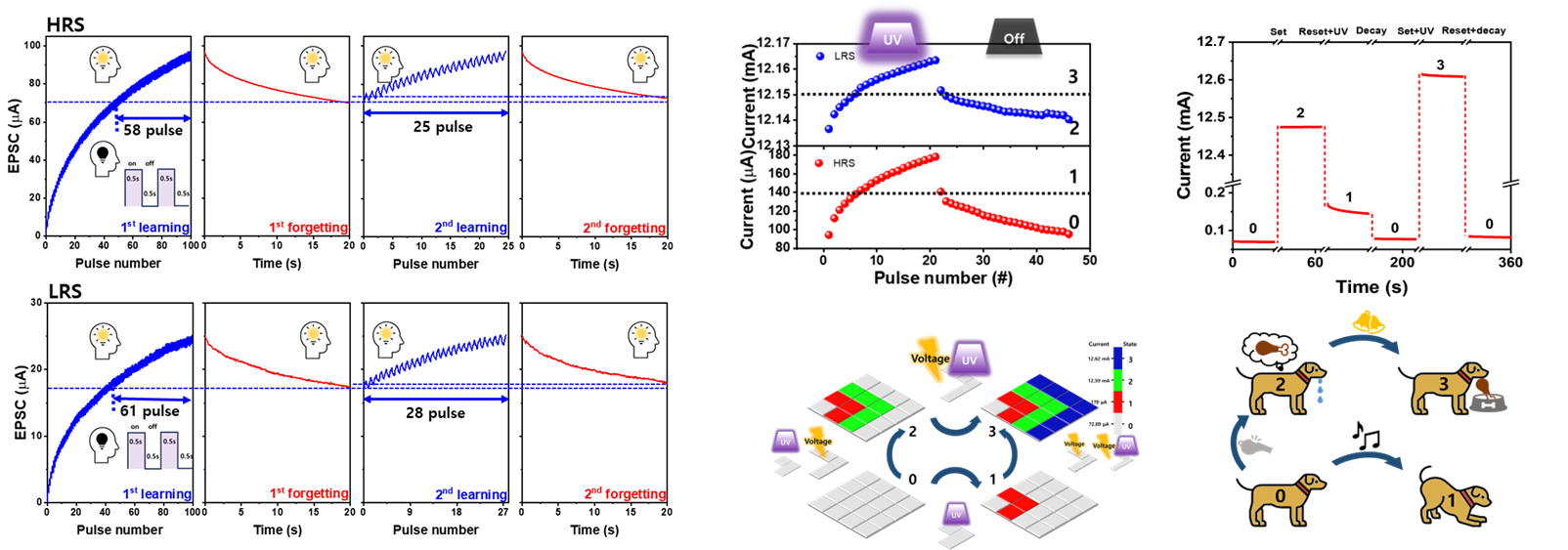
- Demonstrated wavelength-dependent behavior, where shorter wavelengths (UV) reduce learning thresholds and enhance energy efficiency, while longer wavelengths provide gradual control of memory states.
- Observed higher EPSCs (excitatory post-synaptic currents) under higher light intensities, enabling multi-level memory functions.
- Simulations:
- Conducting visual memory simulations on a 3×3 pixel array using UV light of varying intensities to encode memory states and analyze retention over repeated cycles.
- Applications:
- Neuromorphic computing systems, artificial neural networks, and advanced memory devices that mimic biological synaptic functions.

2. Nanomaterials and Thin Films
- Growth Techniques:
- Using Atomic Layer Deposition (ALD) for atomic-scale precision in growing oxide semiconductor films like ZnO, TiO₂, and Ga₂O₃.
- Employing sputtering to produce uniform and scalable films suitable for transistors and transparent conductive layers.
- Developing graphene and carbon nanotube (CNT) nanomaterials via Thermal Chemical Vapor Deposition (CVD) for high-performance electronic and energy devices.
- Research Highlights:
- The thickness and uniformity of films are controlled to enhance optical transparency and electrical conductivity, crucial for photodetectors and solar cells.
- CNT-based films are engineered for their outstanding electron mobility and thermal stability.
- Applications:
- Transparent electronic displays, high-efficiency photodetectors, and wearable energy systems.

3. Neuromorphic Semiconductors
- Devices:
- Focus on designing memristors for combining logic and memory functions in a single device, reducing power consumption and improving performance in neuromorphic systems.
- Optical/electrical synaptic devices simulate biological synaptic plasticity by adjusting resistance and capacitance states under light or voltage stimulation.
- Learning and Forgetting Simulations:
- Devices demonstrate adaptive forgetting, where repeated learning cycles slow down the rate of forgetting, mimicking long-term potentiation in biological neurons.
- Optical synaptic devices show enhanced learning and retention under ultraviolet light stimulation, with multi-level memory storage enabled through repeated learning cycles.
- Applications:
- Realizing neuromorphic AI hardware that can perform brain-like learning and computation with reduced energy demands.

4. Chemical Processes for Oxide-Based Nanostructures
- Materials:
- Developing nanostructures from oxides such as ZnO, TiO₂, and Ga₂O₃ using chemical methods like sol-gel processing, hydrothermal synthesis, and electrodeposition.
- Exploring hierarchical nanostructures for enhanced surface area and optical/electrical properties.
- Focus Areas:
- Using sol-gel techniques to integrate carbon nanotubes into oxide matrices, enhancing photodetection performance.
- Controlling crystallinity and morphology to optimize the device functionality for specific applications like gas sensing and memristors.
- Applications:
- Optoelectronic sensors, memory devices, and flexible electronics with enhanced sensitivity and stability.

5. Advanced Light-Emitting Devices
- Technologies:
- Researching and developing LEDs, Laser Diodes (LDs), and QLEDs with a focus on maximizing light emission efficiency while minimizing power consumption.
- Incorporating quantum dot (QD) materials for improved color purity and brightness in QLEDs, offering superior performance for display technologies.
- Key Challenges:
- Achieving high luminous efficiency while maintaining long-term device stability and reliability.
- Reducing manufacturing costs without compromising device performance.
- Applications:
- High-resolution displays, optical communication systems, medical imaging devices, and advanced lighting solutions.

